After wafers are manufactured, they move to packaging and testing, which ensures chips are reliable and ready for use. Packaging protects chips from moisture, dust, and static electricity and allows them to connect to electronic devices. As Mr. Yang explained, packaging is like “building a house for the chip,” providing safety and stability for everyday use in phones, laptops, AI systems, and medical equipment.
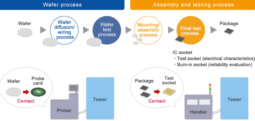
This diagram shows how semiconductor chips are packaged and tested to ensure they function correctly before being shipped.
Testing is equally important.
Chips are checked for speed, energy use, heat tolerance, and signal accuracy. Modern testing is mostly automated, but some processes require human expertise. Proper packaging and testing improve yield, reliability, and performance, which is essential for Taiwan to maintain its global semiconductor leadership.
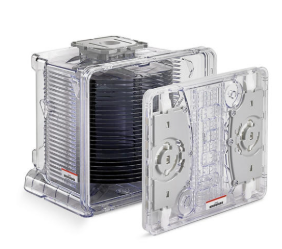
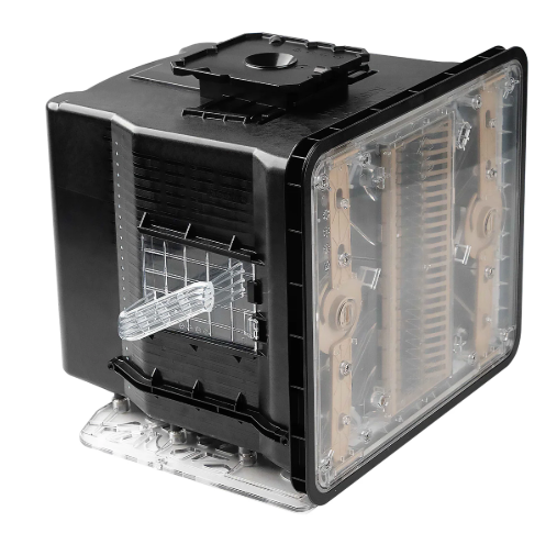
Special containers like FOUPs (Front Opening Unified Pods) and FOSBs (Front Opening Shipping Boxes) are used to store and transport wafers safely. According to Dr. Han, these containers use ePTFE membranes and airtight seals to prevent contamination. Their design, including the number and location of airflow holes, is carefully calculated to maintain optimal dryness and cleanliness.
FOSB container used for wafer shipping
FOUP container used for wafer storage and transport
Packaging and testing also consider sustainability.
Durable, reusable materials reduce waste, while efficient transport minimizes energy use. Taiwan’s semiconductor industry demonstrates how teamwork, innovation, and careful planning unite people, companies, and countries by producing chips that power devices worldwide.
Packaging and testing not only ensure chip quality but also support sustainable and efficient semiconductor production.