Industry Interviews
To better understand Taiwan’s semiconductor industry, we conducted interviews with professionals from different areas of semiconductor field. These interviews helped us learn about history, packaging and testing, and the future development of Taiwan’s semiconductor.
Interview 1 | Dr. Han (EF-Materials Industries)
Dr. Han helped us understand the critical role of materials in the semiconductor industry. He explained that tiny components, like ePTFE membranes, are essential for filtering air, repelling water, and blocking dust in wafer storage and transport. These materials are used in containers called FOUPs (Front Opening Unified Pods) and FOSBs (Front Opening Shipping Boxes), which move wafers safely between machines or factories.
The design of these containers is highly precise. Dr. Han shared how engineers carefully calculate the number and placement of airflow holes and maintain cleanliness through advanced washing and drying methods. Using high-purity water and filtered gases ensures wafers remain uncontaminated. We learned that even small errors in materials or container design could reduce chip quality or production efficiency, showing how important upstream support is for the entire semiconductor process.
Interview 2 | Mr. Yang (Amkor Technology)
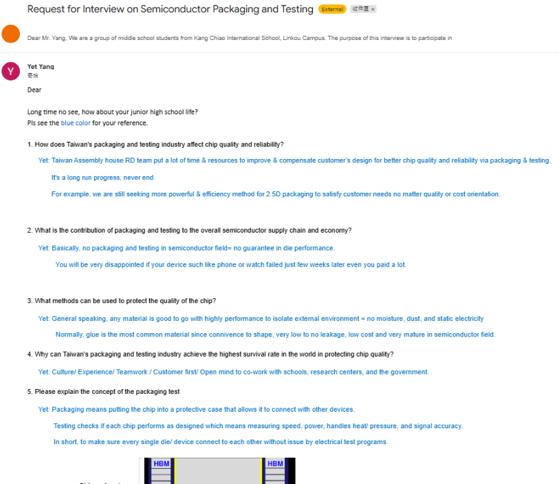
From Mr. Yang, we gained insight into packaging and testing, often called the “last line of defense” for chips. Packaging protects chips from moisture, dust, and static electricity, while testing ensures each chip functions correctly before shipping. He explained advanced techniques like 2.5D and 3D packaging, which integrate multiple chips into one package, improving performance but also increasing testing complexity.
Automation plays a large role, but human expertise is still needed for special tests and equipment setup. Mr. Yang also described challenges the industry faces, including high costs, global competition, and sustainability concerns like water and energy use. Despite these pressures, Taiwan’s packaging and testing companies remain leaders due to their experience, teamwork, and innovation, often collaborating closely with universities, research centers, and international partners.
Interview 3 | Dr. Yuan (Nanya Plastics)