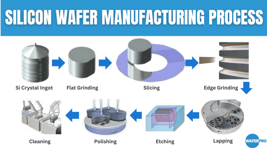
After design, chips move to wafer manufacturing, also called fabrication. This stage builds the circuits on silicon wafers through many precise steps, including photolithography, etching, chemical vapor deposition (CVD), physical vapor deposition (PVD), and chemical mechanical polishing (CMP). These steps are repeated dozens or even hundreds of times to create multilayer circuits.
Picture from Waferpro.com
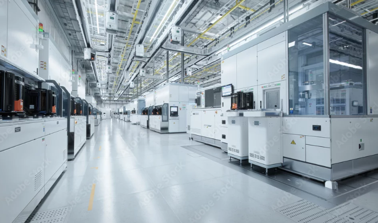
Cleanliness is essential.
Dr. Yuan from Nan Ya Plastic explained that wafers must be produced in high-level cleanrooms, where air is filtered and monitored constantly. Even a tiny dust particle can ruin a chip, showing how sensitive this process is. Manufacturing also requires huge amounts of water and electricity. For example, a 12-inch wafer fab may use 100,000–200,000 tons of water daily, mostly recycled, and electricity needs can reach 1.9 GW, nearly as much as a medium-sized power plant. Taiwan’s leading companies, like TSMC, are investing in renewable energy and energy-saving technologies to reduce carbon emissions and maintain sustainability while producing high-tech chips.
A semiconductor cleanroom where wafers are manufactured in a controlled environment to prevent contamination.
The precision of these processes ensures high-quality chips, and the careful use of resources demonstrates how Taiwan contributes to global technology while respecting environmental responsibilities.